SEM (Scanning Electron Microscope)
SEM (Scanning Electron Microscope)
High-Resolution Surface Imaging and Analysis System
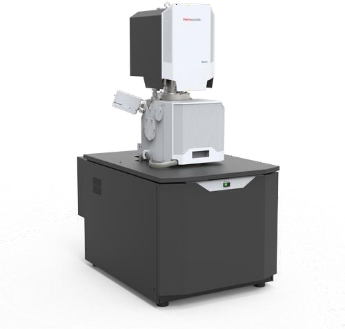
Thermo Scientific Apreo S device
Description
SEM (Scanning Electron Microscope) operates on the principle of utilizing interactions that occur when electrons emitted from a field emission gun (FEG) are directed onto the surface of the material to be examined. In a scanning electron microscope, image formation is fundamentally based on collecting and analyzing signals resulting from physical interactions between the electron beam and the surface of the sample.
Application Areas
- Conductive/Insulating Materials
- Biological Materials
- Geological Samples
- Textile Products
Device Configuration and Technical Specifications
Model: Thermo Scientific Apreo S
Detectors: ETD (SE), T1 (In-Column BSE), T2 (In-Column SE), retractable BSE, EBIC, STEM, LVD, EDS
Sample Chamber Inner Diameter: 340 mm
Vacuum: High vacuum – Low vacuum
Electron Source: Schottky Field Emission Gun (FEG)
Please log in to the Erasis system to submit an analysis request.


