SPM and AFM Microscope
Information About Scanning Probe Microscope Systems

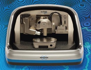
Bruker Dimension Edge AFM/SPM system
Description
Scanning Probe Microscopy (SPM) includes high-resolution imaging techniques such as Scanning Tunneling Microscopy (STM) and Atomic Force Microscopy (AFM). The Bruker Dimension Edge SPM is capable of analyzing conductive, semiconductive, and non-conductive samples in both air and liquid environments.
Differences Between STM and AFM
While STM can only image the surface structure of conductive or semiconductive samples, AFM can also image non-conductive samples and map surface topography with high precision.
Operating Modes
- Contact Mode: The probe tip remains in constant contact with the surface.
- Non-Contact Mode: The probe detects interatomic forces without touching the surface.
- Tapping Mode: The probe intermittently touches the surface in a controlled manner to perform measurements.
Available Analyses
- Surface morphology and topography analyses
- Coating/film thickness measurement
- Surface roughness characterization
- Surface adhesion and phase mapping
- Hardness and elasticity analysis via nanoindentation
- Localized mechanical property mapping
- Electrical conductivity and magnetic field imaging
- Sample examination in liquid environments (e.g., cells)
Device Information
Brand: Bruker
Model: Dimension Edge with ScanAsyst
Scan Area: Maximum 90 µm x 90 µm
AFM SPM Nanoanalysis Surface Mapping
Please log in to the Erasis system to submit an analysis request.


